- Home
- Automated Solutions
- High Throughput Inkjet Printing Technology in Printed Electronics
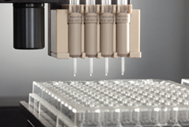 Sample preparation is the critical step in HTS and becomes more challenging when using IJP. Microdrop Technology GmbH in Germany possesses excellent IJP, enabling reproducible dispensing of droplets at microscopic scale from a wide range of materials. Importantly, it unprecedentedly integrates the IJP into the pipettes, making it possible to automatically fill, print, recycle the materials which are prepared in 96-MTP. By configuring a highly accurate positioning system and by employing an in-flight dispensing function, it can print many solutions precisely and swiftly, and prepare high quality high-throughput samples.
Three elements are required for HTS, which include model building, automatic HT sample preparation and sample analysis. Among them, automatic HT sample preparation is critical.


Fig 1: Three elements for HTS
Below is the workflow of HT sample preparation and screening by using microdrop Professional inkjet printing platform. Mouse over the blocks to see an example and videos.


In the workflow above, we need to print many solutions (A-Z). If using the traditional inkjet printing platforms, it needs much more manual operations to clean the heads, change the solutions, and reposition etc, which will lead to low efficiency and unnecessary material consumption and certainly not fit for HT sample preparation. Based on the advantages listed in the following table, microdrop Professional inkjet printing platform is ideal for automatic HT sample preparation.
| Advantages | Descriptions |
| Multi-channel | Support up to 8 dispenser heads |
|---|---|
| Auto-pipette | Based on 96-MTP, it is able to change, print, recycle solutions, clean the dispenser head and can print many solutions at one time. |
| Ultra-small volume | Diameter down to 30 μm, volume down to 20 pl, saving materials |
| High accuracy positioning | Positioning accuracy: ±5μm; Repetition accuracy: ±1μm, ensuring sample quality |
| Good stability | Droplets size variation smaller than ±1%, ensuring sample quality |
| In-flight dispensing | Dispensing fast and accurately |
| Automatic dispensing | All procedures can be completed automatically via software programming. |
| Easy operation | Easy to adjust pressure, set parameters and clean dispenser heads |
Thanks to the advantages, such as self-luminous, low power, light weight, wide viewing angle, fast response and high image quality, polymer light emitting diode (PLED) is widely used in display and lighting fields and is a fast-developing and highly prospective topic in printed electronics. However, the limitation on the cost, largesize, full color, and other factors, will be more obvious ifusing the traditional deposition techniques. IJP is not only expected to solve these problems, but also has the great potential to print PLED anode, cathode and TFT structures. Thus it is an ideal preparation technology for PLED manufacturing.
Using IJP to produce a uniform, stable and highly luminescent PLED film, it requires screening and optimization for various parameters which affect the film quality and properties [Fig. 2].
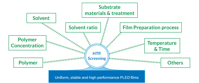
Fig. 2: Screening and optimization for various parameters
In this case [1, 2], researchers synthetized red, green and blue luminescent materials, namely PPV-PPE, PPV and PFP, respectively [Fig. 3]. After dissolving these materials in appropriate solvents, their solutions are usedfor subsequent dispensing. Films are formed after drying. Researchers studied carefully the effects of polymer concentration, solvents, boiling point difference and ratio of mixed solvents, dot spacing, substrate temperature and so forth on the uniformity of polymer films [Fig. 4] thus screened for the most optimized parameters [Fig. 5].
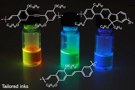
Red:PPV-PPE
Green:PPV
Blue:PFP
Fig. 3: Red, green and blue luminescent materials
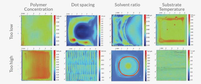
Fig. 4: PLED films formed under different conditions

Fig. 5: Uniform PLED film after combinatorial screening
Reference
【1】 A. Teichler, et al., European Polymer Journal 49, 2186-2195, (2013).
【2】 A. Teichler, et al., Thin Solid Films 519, 3695-3702 (2011).
Organic photovoltaic (OPV) has been receiving increasingattention because of itslow cost, simple process, low environmental concern and the capability of manufacturing flexible battery. Currently, the blend heterojunction OPV can achieve the higher photoelectric conversion efficiency. This so-called heterojunction is simply prepared by blending electron-donor and electron-acceptor materials to form the film. To obtain high performance solar cells, optimization for the blending of raw materials is necessary to produce a film with low energy gap and wide absorption spectrum.
Using microdrop Professional inkjet printing platform, it is very convenient to do HTS for optimization of polymer materials, polymer combinations, and preparation conditions . In this case3, researchers screened different blend conditions for three conjugated polymers and PCBM [Fig. 6] by studying the absorption spectrum and surface roughness of the films formed via HTS. They finally obtained the optimal blending condition, making the film with best photovoltaic performance.
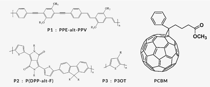
Fig. 6: Three conjugated polymers and PCBM
Combinatorial screening process for the best blending condition
(1)As a good electron acceptor, PCBM is usually used in OPV. So first of all, it is necessary to consider the surface morphology of various conjugated polymers after blending them with PCBM. , . Formation of a rough surface from blending of P1 and PCBM by atomic force microscope (AFM) [Fig. 7] is not beneficial to electron transport. However, the respective blending of P2, P3 and P2/P3 with PCBM can form smooth and uniform films. Thus, it is important that use of conjugated polymers of P2 and P3 is preferred when mixed with PCBM.
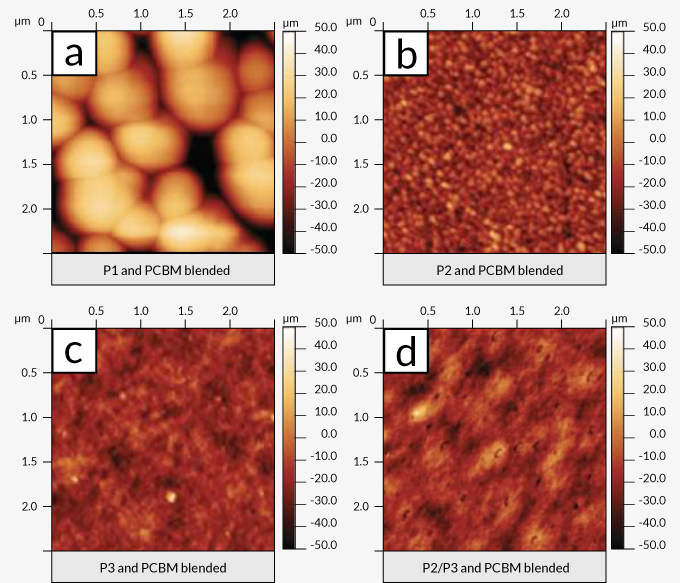
Fig. 7: AFM images for prepared films by blending P1, P2, P3, P2/P3 with PCBM respectively
Conjugated polymers P2 and P3 have their own absorption spectra. Blending will broaden the absorption spectrum and improve the photoelectric efficiency. By measuring the absorption spectrum of films formed under various blend ratios of P2 and P3 [Fig. 8], it is found that the ratio of 4/6 for P2/P3 will give the best absorption spectrum.
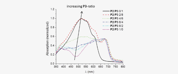
Fig. 8: Absorption spectrum for different blend ratio of P2/P3
(3)After that, they blend P2/P3 with a fixed ratio of 4/6 and then blend P2/P3 with PCBM in different combination ratios. By measuring the absorption spectrum and emission intensity [indirectly implying the electron-hole recombination rate] of the films [Fig. 9], it is found that P2/P3/PCBM film with the ratio of 4/6/30 has the optimal absorption spectrum and lowest emission intensity.
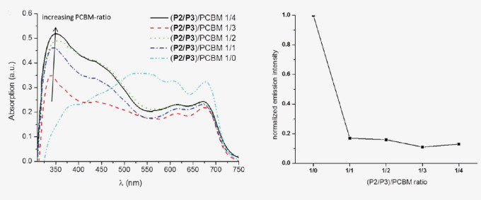
Fig. 9: Absorption spectrum (a) and emission intensity (b) of the films prepared under different blending ratios of P2/P3 and PCBM (P2/P3 is mixed at a ratio of 4/6)
(4)Optimized results: P2/P3/PCBM film has the best performance at a blending ratio of 4/6/30.
References
【3】 A. Teichler, et al., ACS Comb. Sci. 15, 410-418 (2013)